13th December 2015 by Pambos Palas
Analogue to Digital Conversion [PART 6 – AVR]
Having briefly covered the general theory behind Analogue to Digital Conversion (see Signals, Sampling, Aliasing, Resolution, Accuracy), we will now look at an actual implementation. In this particular case we will be using an embedded Microprocessor Unit (MCU), specifically the Atmel Atmega32, as our platform. For anyone who has had experience with this embedded processor or a similar one, you will know that they are very powerful units with great flexibility – for further information, please have a look at the datasheet.
It will be assumed that the hardware is setup already, and any considerations on that front won’t be covered in this particular post, instead, we will focus on the software setup to get an analogue to digital conversion going. Although this post will act as a guide for a particular application, I would recommend reading the relevant section of the datasheet if you are looking to implement this yourself as there are many things to look out for and these vary depending on application.
In our case, we will be looking at a temperature sensor, the TMP37 (Datasheet), which is intended for measurements between 5°C and 100°C. At ambient temperature, assumed here to be 25°C, the output is at 500mV, and this sensor provides and output scale factor of 20mV/°C.
Before jumping into it, it is worth having a look at the overview of the converter and what it can do. As specified in the datasheet, the converter on the Atmega32 includes:
- 10-bit Resolution
- 0.5 LSB Integral Non-linearity
- ±2 LSB Absolute Accuracy
- 13 µs – 260 µs Conversion Time
- Up to 15 kSPS at Maximum Resolution
- 8 Multiplexed Single Ended Input Channels
- 7 Differential Input Channels
- 2 Differential Input Channels with Optional Gain of 10x and 200x
- Optional Left adjustment for ADC Result Readout
- 0 – VCC ADC Input Voltage Range
- Selectable 2.56V ADC Reference Voltage
- Free Running or Single Conversion Mode
- ADC Start Conversion by Auto Triggering on Interrupt Sources
- Interrupt on ADC Conversion Complete
- Sleep Mode Noise Canceler
We can see that 8 single-ended input channels are available to us, and these are included in PORTA on PIN0 – PIN7 (shown in Figure 1). So, having powered our sensor with 5V, we can connect the output to any of our analogue pins – here we will assume PINA0.
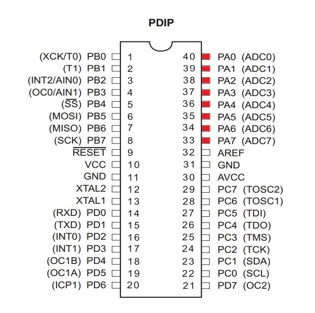
Figure 1 – Atmega32 PDIP pin layout with analogue input pins shown in red.
So once the wiring is complete, we need to initialise the ADC with the required settings that we want for this application. To do that, we need to set a number of special registers to have values according to the settings that we require. These will be detailed below along with a short description of the significance.
ADMUX – ADC Multiplexer Selection Register
The first register we will be setting is the ADMUX register, which serves several purposes. The bits it includes, along with their initial values can be seen in Figure 2 below.

Figure 2 – ADMUX Register.
The first bits we need to set are bits 7-6 (REFS1 and REFS0). The combination selected for these two bits will determine the reference voltage to be used in our application. The choices are shown in Figure 3 below.
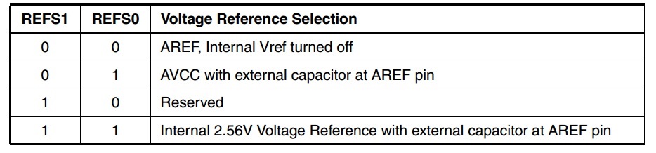
Figure 3 – Reference Voltage Selection.
If both bits are set to 0, we can set the voltage reference ourselves by applying it to the AREF pin. Other choices are using AVCC (which should be between 2.7V – 5.5V), or if we want we can choose a third option which is to use an internal 2.56V Voltage reference. Looking at our application, we know that we are looking at a maximum temperature of 100°C. This would give us 2000mV according to the datasheet, and we would therefore not expect anything above 2.56V. This seems like a good choice, as it is for the most part in line with our range of voltages that we will expect. If we go for anything higher, we would be reducing the accuracy of the measurement as we would lower the resolution (see Part x) [LINK]. If we wanted to be even more accurate we could have opted to set the voltage ourselves to just over 2V, but for what we need this is probably not worth it given the accuracy of the sensor.
Since we have 10 bit resolution, we will have 2^10 = 1024 steps, ranging from 0 for GND to 1023 for VREF (2.56V). Therefore each step will be 2.56/1024 = 2.5mV, or, since the output scale factor is 20mV/°C, we are looking at steps of 0.125°C. Since the accuracy of the sensor is anyway stated to be ±2°C, this should be more than good enough for our application (in fact using 5V as a reference voltage is more that fine as well, but since we have 2.56V readily available we might as well use it).
Moving on to bit 5 (ADLAR), we will set this to 1 to left adjust the result. This will be explained later in detail when we look at reading the result, but basically this determines how the result is given to us when the conversion is complete. This is a matter of preference, but it should be taken into account when writing the code to interpret the result.
Finally, bits 4-0 (MUX4-MUX0) are used to determine which combination of analog inputs are connected to the ADC, and can also be used to set gain. This is done according to the table shown below in Figure 4.
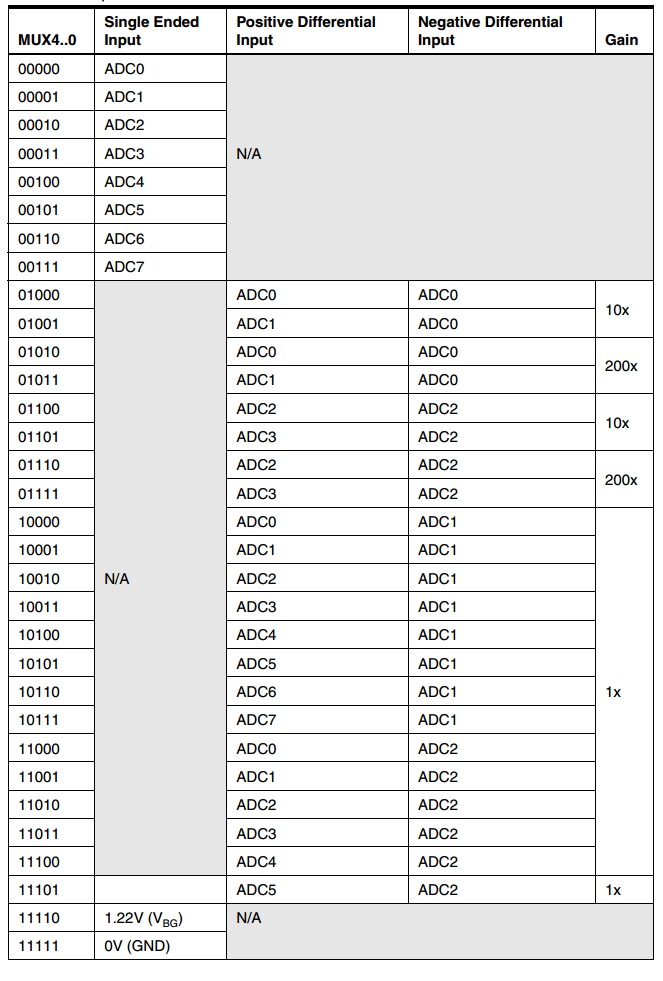
Figure 4 – MUX bits in ADMUX register.
Since we are only looking at single ended conversion for this application, and we are connected on PINA0, we can keep the MUX bits set to 0 to select ADC0. An example where differential input could be used with operational gain is in the measurement of strain using a strain gauge in a Wheatstone bridge configuration – there, a very small difference in voltage has to be detected.
ADCSRA – ADC Control and Status Register A
The second register we will be setting is the ADCSRA register. The bits it includes, along with their initial values can be seen in Figure 5 below.
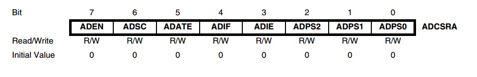
Figure 5 – ADCSRA Register.
We will not be setting bit 7 (ADEN) just yet, as this is the ADC Enable. Setting this to 1 will enable the ADC, but first we will finish with the initialisation. This will be turned on just before we are ready for the first conversion.
Similarly, bit 6 (ADSC) will be set later, as this is the bit that will instruct the MCU to start the conversion. Setting this to 1 will start the conversion, and when the conversion is finished it will be set to 0 automatically. It should be noted here, that the first conversion will take 25 ADC clock cycles (not to be confused with the MCU clock cycles – see below), and subsequent conversions will take 13 ADC clock cycles.
Bit 5 (ADATE) is the ADC Auto Trigger Enable and is beyond the scope of our application. Essentially, setting this to 1 will enable the ADC to automatically start a conversion upon a trigger signal. Here we will be starting the conversion manually.
Bit 4 (ADIF) is very important as it will tell us when an ADC conversion is complete and the result is ready to be read. We will not do anything with it now, but will keep checking it after we start a conversion so that we know when the conversion is finished.
Bit 3 (ADIE) is used to enable interrupts and is beyond the scope of our application.
So finally, the only bits we will be setting at this point are bits 2-0 (ADPS2-ADPS0). These select the ADC Prescaler that will be used. At this point, it’s important to note that the MCU’s clock speed is quite high in relative terms for the ADC circuitry. According to the datasheet, the internal circuitry requires an input clock frequency between 50kHz and 200kHz to get maximum resolution. If we assume that our MCU has a clock speed of 8MHz, then it is significantly higher and we have to reduce it. This is where the prescaler comes in. We use the prescaler to divide the MCU clock speed by a certain factor so that it falls within an acceptable range. The various settings available to us can be seen in the table in Figure 6 below.

Figure 6 – Prescaler Settings.
So if our MCU is running at 8MHz, and we are aiming for something between 50kHz and 200kHz, then it would make sense to divide it by 64. This would give us: 8000/64 = 125kHz, which is acceptable. Therefore we will be setting bits ADPS2 and ADPS1 to 1.
This is it for the settings of the ADC. So we can already write our initialisation function which will look something like this:
[code language=”cpp”]
void ADC_init (){
ADMUX = _BV(REFS1) | _BV(REFS0) | _BV(ADLAR); // ADMUX = 0b11100000
ADCSRA = _BV(ADPS2) | _BV(ADPS1); // ADCSRA = 0b00000110
}
[/code]
Starting a Conversion
Now that we are ready, we can write a function that will perform a conversion and give us the result.
[code language=”cpp”]
uint16_t get_adc_result(){
ADCSRA = _BV(ADEN); //Enable ADC
ADCSRA = _BV(ADSC); //Start conversion
/* Time for conversion:
First conversion = 25 ADC clock cycles (0.16 ms)
ADC Clock speed = (8 x 10^6) / 64 = 125,000 Hz
Period = 1 / 125,000 = 0.000008 seconds
= 8 us (microseconds)
*/
loop_until_bit_is_set(ADCSRA, ADIF); // Wait until the conversion is finished.
uint16_t result = (ADCH << 2) | (ADCL >> 6); // Read the final result.
ADCSRA &= ~_BV(ADEN); //Disable the ADC
return result;
}
[/code]
All the lines should be self-explanatory, as the registers have been described above, with the exception of ADCH and ADCL. These are used when we read the result, and as you may have determined, they store the result. The necessity to have two registers to store the result is due to the ADC having a 10-bit resolution and the MCU only being able to support 8-bit registers. Indeed, only one of the registers is fully used to store the result, and only 2 bits from the other register are used for the rest.
This is where bit 5 (ADLAR) of the ADMUX register comes into play, as this determines how the result will be stored in the two registers ADCH and ADCL. We set it to 1, to left adjust the result, but this is a matter of preference. Figure 7 below illustrates how the result is presented to us, and how the ADLAR bit will affect it.
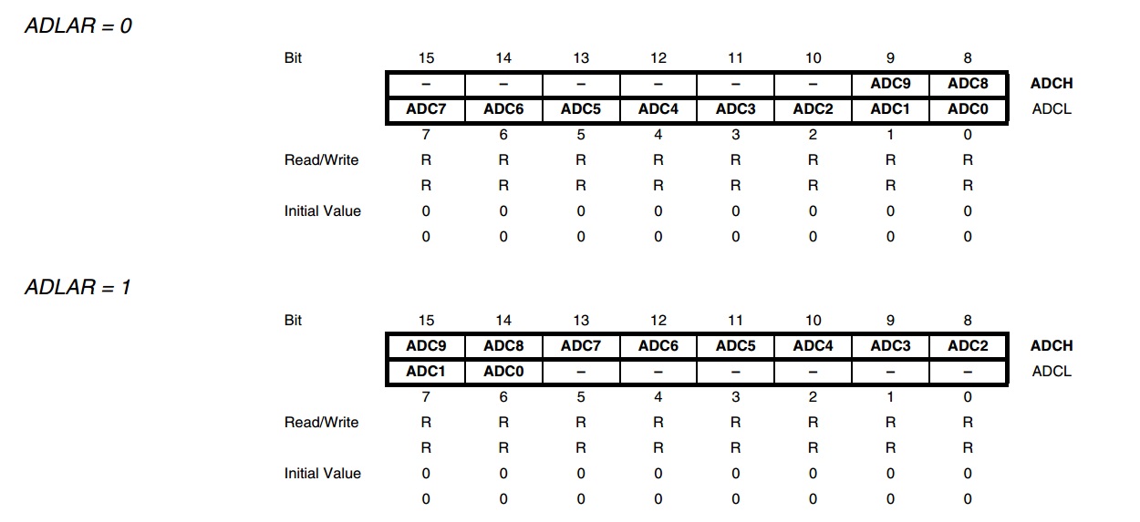
Figure 7 – ADCH and ADCL.
It should be noted, that if 10-bit resolution isn’t required, then we can simply read ADCH (in our case where it is left adjusted) and ignore ADCL.
This is it for this blog post. If anyone has any questions or comments about any of this, please leave a comment below and I will try to respond as soon as possible.